The goddess of flexible electronics, academician Bao zhe Nan, three hits in a row in science!
Skin like and elastic electronic devices compatible with biological tissues and able to adapt to body movement are ideal choices for skin sensors, body area networks and implanted bioelectronics. The development of polymer electronic materials greatly promotes the development of flexible and scalable electronic materials. At present, bio integrated electronics mainly adopts hybrid method to integrate rigid and scalable components, but this method will lead to local stress at rigid flexible interface and mechanical properties mismatch when contacting with biological system. In order to construct a fully elastic sensing system, elastic chip should be used to replace the rigid chip which is in direct contact with the biological system. However, compared with silicon-based devices, due to the lack of a universal micro / nano fabrication method for skin like and elastic circuits, the device density is low and the parallel signal recording and processing ability is limited.
Recently, Stanford University s Bao jenan team proposed a single-chip optical micro lithography process, which directly patterned elastic electronic materials through continuous UV triggered solubility modulation. The researchers made transistors with a channel length of 2 microns and a density of 42000 transistors per square centimeter. Based on this method, an elastic circuit including XOR gate and half adder (both are basic components of arithmetic logic unit) is constructed. This process provides an idea for the wafer level fabrication of complex, high-density, multilayer elastic circuits, and its performance is comparable to that of rigid circuits. The study was published in the latest issue of science with the title of monolithic optical microscopy of high-density elastic circuits . It is understood that this is academician Bao zhe Nan s third science from 2020 to now�� Two consecutive articles science , flexible electronic goddess, academician Bao Zhenan s achievements in 2020)
[simplified lithography process]
An efficient photoinitiated carbene insertion reaction was used as a general crosslinking method for semiconductor and insulating polymers (Fig. 1E). In addition, polyethylene glycol acrylate (pegdma), which is sensitive to ultraviolet light, is introduced to realize the double network mediated direct photolithography (no chemical modification) of conductive polymer. The device can be manufactured in four direct lithography steps without additional protection, etching, transfer or lamination processes (Figure 1F). The cross-linking based patterning strategy makes each layer stable and chemically resistant, allowing wafer scale layer by layer deposition.
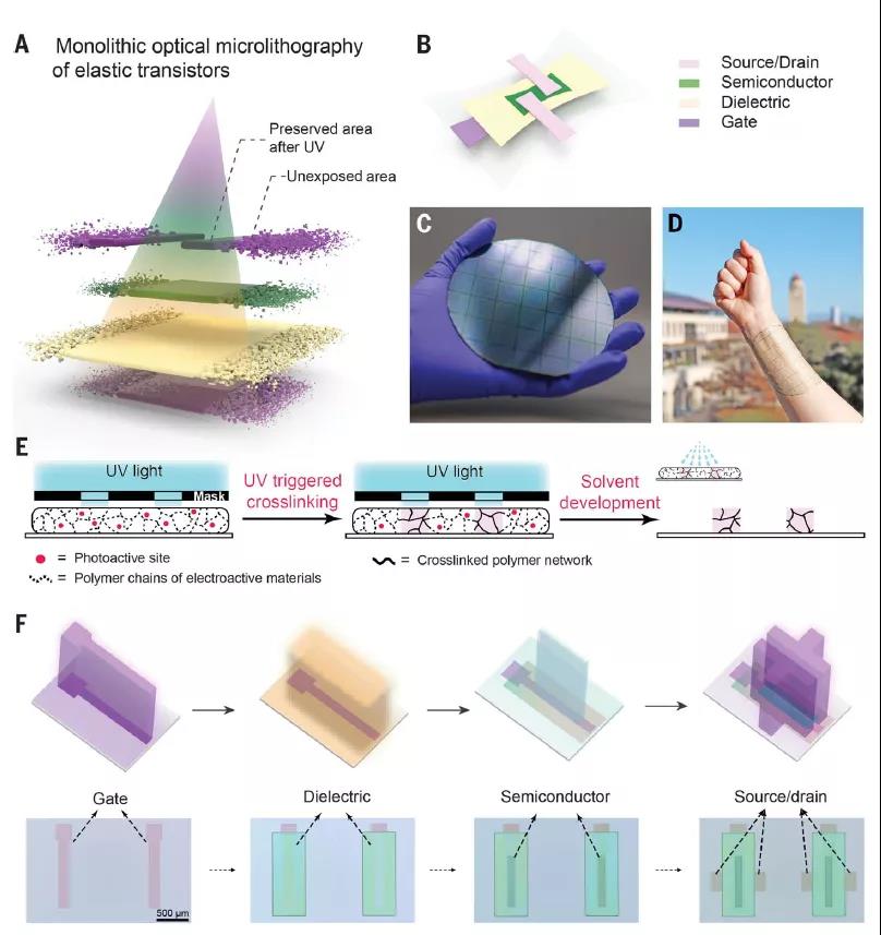
Fig. 1 high density elastic circuit for single chip lithography
[solubility adjustment]
The solubility of PEDOT: PSS can be achieved by embedding physical crosslinking conductive network into covalently crosslinked pegdma network. The strong interaction between PEDOT and PEG linker results in the transition of the microstructure of PEDOT: PSS from core-shell structure to longer chain, thus forming the first conductive network (Fig. 2a). After UV irradiation (365 nm), the second network was formed by rapid radical polymerization of polyethylene glycol modified by dimethyl acrylate (DMA). The strong intermolecular interaction between the two networks makes the area exposed to UV resistant to water, while the unexposed area is still water-soluble. This photopatterning ability is closely related to the ratio of pegdma / PEDOT. Insufficient pegdma will lead to poor corrosion resistance of the film, while excessive pegdma will lead to crosslinking before UV exposure (Fig. 2a, b). With the increase of PEG linker, the interchain coupling between PEDOT molecules is stronger, and PEDOT is more stable ��-�� The stacking distance decreases gradually and larger grains are formed (Fig. 2c, d). By adjusting the appropriate ratio (1.15:1 pegdma / PEDOT), the resolution of 2 �� M (Fig. 2E, f). In addition, the conductivity of PEDOT: PSS was greatly improved by adding pegdma.
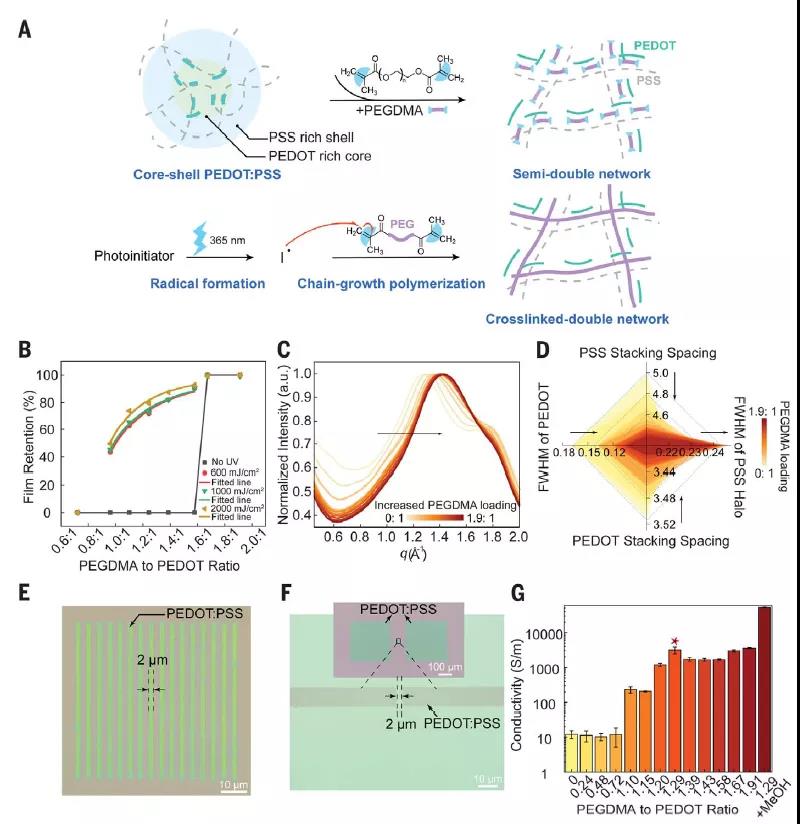
Figure 2. Double network mediated direct photolithography of conducting polymers
[improve resolution, ensure mobility]
A bifunctional trifluoromethyl substituted diazirine crosslinker was introduced (Fig. 3a). Carbene species formed by rapid photodegradation can undergo a cleaning reaction specific to the unconjugated bonds on the side chains of conjugated polymers, resulting in an increase in molecular weight, resulting in UV induced solubility regulation. The cross-linking reaction is aimed at the non conjugated side chain without destroying the conjugation on the main chain. The degradation of charge transfer characteristics of semiconductor polymer is prevented. The photocrosslinking efficiency varies with the molecular weight of the polymer (Fig. 3b). The resolution can be further improved by reducing the molecular weight distribution. In addition, the higher the content of crosslinker, the lower the mobility of the film (Fig. 3e)
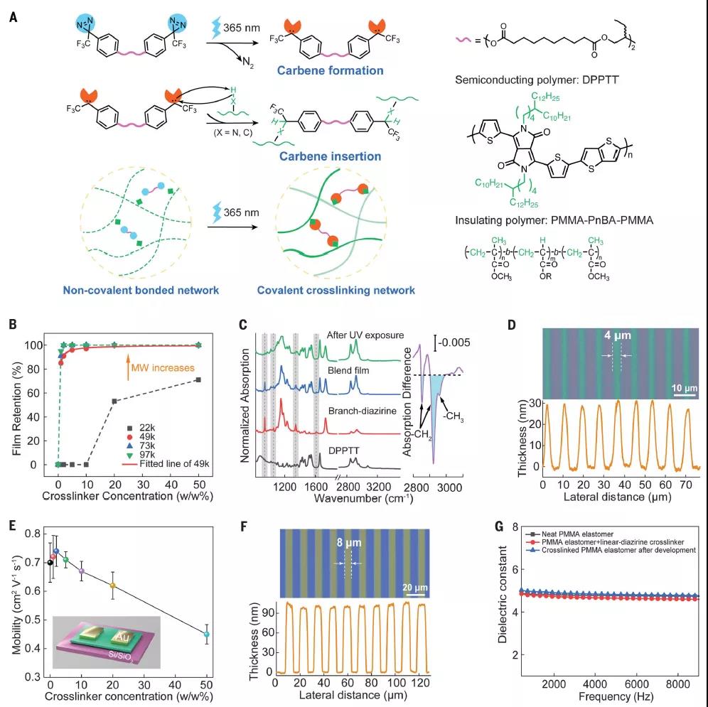
Fig. 3 direct photolithography of carbene mediated semiconductors and insulating polymers
High density transistor array
The researchers fabricated an all polymer elastic transistor array with 10000 transistors on a 0.238 cm2 substrate (FIG. 4A, b). The device density is as high as 42000 transistors per square centimeter, which is more than 100 times of the density of the array prepared by mask etching process. Device channel length 2 �� m. Width 40 �� m�� The switching ratio is 104 and the off state current is as low as 0.5 Na (Fig. 4C). Subsequently, 10 samples were prepared �� The average saturation mobility is 0.255 M2 V �C 1 s �C 1 (Fig. 4F). The device yield is 98.5%, and the standard deviation is only 3.76% (Fig. 4G). The distribution of threshold voltage (Vth) is 0.61 �� 45 V (Fig. 4h), which is only 1.5% of the operating gate source voltage window (30 V). At 100% strain parallel to and perpendicular to the charge transfer direction, the transistor array has no visible cracks or delaminations (Fig. 4J), which confirms that each layer has excellent mechanical properties. Its electrical properties are stable along the charge transport direction and under 100% strain. The mobility is kept at 88% of the original value and the threshold voltage is close to 0V (Fig. 4I). In the vertical direction, the mobility decreases slightly. Under 50% strain in both directions, it can withstand 1000 times of repeated tension without obvious change in electrical properties (Fig. 4K).
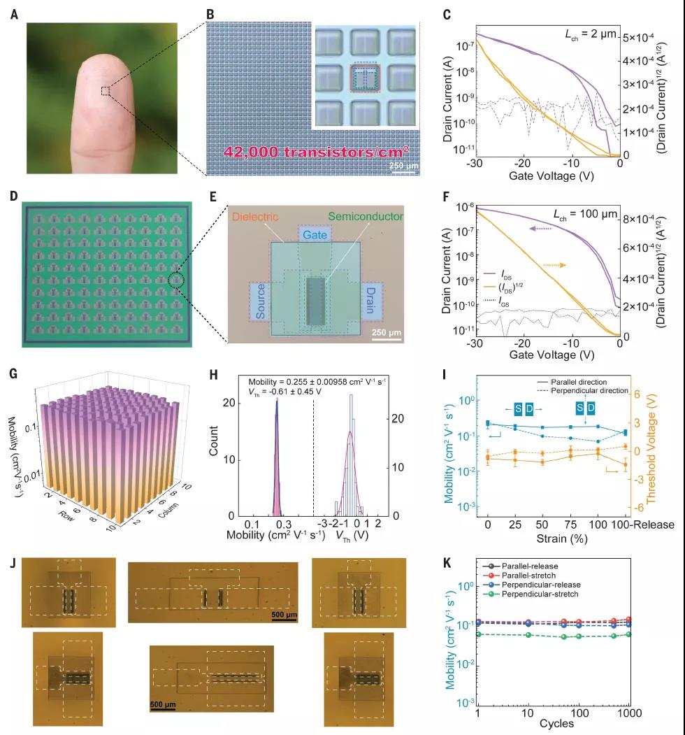
Figure 4 high density uniform elastic transistor array
Flexible integrated circuit
Finally, the inverter and NAND gate are fabricated. The channel length of the flexible inverter is only 10 �� m. The spatial resolution is one order of magnitude higher than that reported previously. When the logic input status is 0 and 1, the inverter can also work normally under 100% strain (Fig. 5b). The normal operation of more complex logic XOR gates (24 transistor integrated) and half adders (30 transistor integrated) shows the uniformity and high yield of all cell devices.
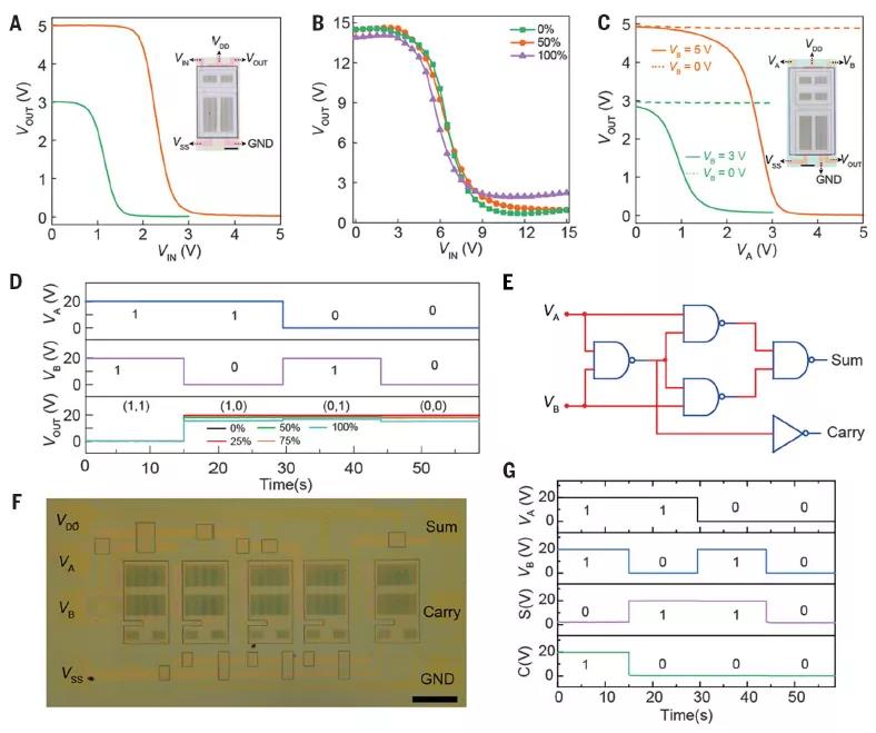
Figure 5 elastic function circuit
Conclusion: an efficient photo initiated carbene insertion reaction is used as a general crosslinking method for semiconductor polymers and insulating polymers. At the same time, ultraviolet sensitive polyethylene glycol acrylate (pegdma) was introduced to realize the double net mediated direct photolithography of conductive polymer. The channel length is 2 �� The density is up to 42000 transistors per square centimeter. Based on this method, an elastic circuit including XOR gate and half adder (both are basic components of arithmetic logic unit) is constructed. This process provides an idea for the wafer level fabrication of complex, high-density, multilayer elastic circuits, and its performance is comparable to that of rigid circuits.
This information is from the Internet for academic exchange only. If there is any infringement, please contact us to delete it immediately
+86-18915413828(WhatsApp&WeChat)
Previous�� Zhejiang University Sc
Next�� Nature communications


